Metal-assisted chemical Etching (MacEtch)
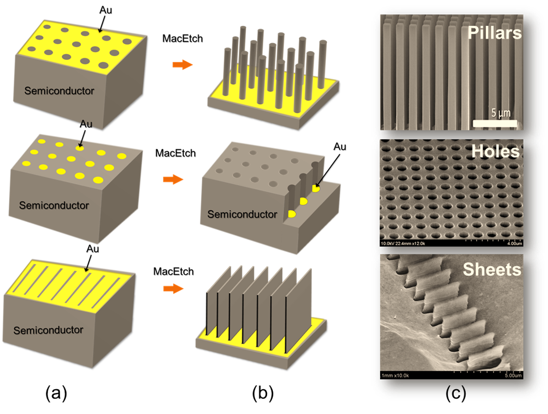
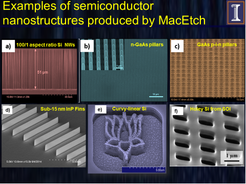
Metal-assisted Chemical Etching (MacEtch) is a novel nanofabrication method we have discovered (Appl. Phys. Lett. 77, 2572 (2000) and Patent US#6,790,785.) originally to produce porous silicon and then developed to produce extremely high aspect ratio semiconductor nanostructures including Si, Ge, GaAs, InGaAs, InP, SiC, GaN, Ga2O3 homo- and hetero-junctions. It uses noble metal (such as Au, Pt and Ag) deposited on the surface of a semiconductor (e.g. Si) as a catalyst to catalyze the hole (h+) generation from an oxidant (such as H2O2) in an acidic (or basic) solution (such as HF) to induce local oxidation (Si + 4h+ --- Si4+) and reduction (2H+ + 2e- --- H2) reactions. This results in the removal of semiconductor materials without net consumption of the metal. Under controlled consitions, the reactions occur only at the interface between metal and the semiconductor, under controlled etching conditions. As a result, metal descends into the semiconductor as the semiconductor is being etched right underneath, acting as a negative resist etch mask. When the catalyst metal is patterned in any shape and dimension, the pattern can be engraved into the semiconductor to produce micro and nanostructures including arrays of pillars for energy harvesting and storage, vias for photonic crystals, and arbitrary shape and patterns for applications including metamaterials. MacEtch is essentially a wet etching method yet produces anisotropic high aspect ratio semiconductor micro and nanostructures without incurring lattice damage.
Variations of MacEtch include:
- Our Publications on MacEtch:
- H.-C. Huang, M. Kim, X. Zhan, K. Chabak, J. D. Kim, A. Kvit, D. Liu, Z. Ma, J.-M. Zuo, and X. Li, "High Aspect Ratio Ga2O3 Fin Arrays with Low-Interface Charge Density by Inverse Metal-Assisted Chemical Etching," ACS Nano, accepted. DOI: 10.1021/acsnano.9b01709.
- J. D. Kim, M. Kim, C. Chan, N. Draeger, J. J. Coleman, and X. Li, "CMOS Compatible Catalyst for MacEtch: Titanium Nitride Assisted Chemical Etching in Vapor Phase for High Aspect Ratio Silicon Nanostructures," ACS Appl. Mater. Interfaces, accepted (2019).DOI: 10.1021/acsami.9b00871
- M. Kim, H.-C. Huang, J. D. Kim, K. D. Chaback, A. R. Kumar, W. Zhou, and X. Li, "Nanoscale Groove Textured beta-Ga2O3 by Room Temperature Inverse Metal-assisted Chemical Etching and Photodiodes with Enhanced Responsivity," Appl. Phys. Lett. 113, 222104 (2018).[pdf]
- M. Kim, S. Yi, J. D. Kim, X. Yin, J. Li, J. Bong, D. Liu, S-C. Liu, A. Kvit, W. Zhou, X. Wang, Z. Yu, Z. Ma, and X. Li, "Enhanced performance of Ge photodiodes via monolithic antireflection texturing and α-Ge self-passivation by inverse metal-assisted chemical etching," ACS Nano, 12 (7), pp 6748-6755 (2018).[pdf]
- J.D. Kim, M. Kim, L. Kong, P. Mohseni, S. Ranganathan, J. Pachamuthu, W.K. Chim, S.Y. Chiam, J.J. Coleman, and X. Li, "Self-Anchored Catalyst Interface Enables Ordered Via Array Formation from Sub-micron to millimeter Scale for Poly- and Single-Crystalline Silicon," ACS Appl. Mater. Interfaces, 10 (10), pp 9116–9122 (2018). [pdf]
- L. Kong, Y. Song, J.D. Kim, L. Yu, D. Wasserman, W.K. Chim, S.Y. Chiam, and X. Li, "Damage-Free Smooth-Sidewall InGaAs Nanopillar Array by Metal-Assisted Chemical Etching," ACS Nano, 11 (10), pp 10193-10205 (2017).[pdf]
- J. D. Kim, P. K. Mohseni, K. Balasundaram, S. Ranganathan, J. Pachamuthu, J. J. Coleman, and X. Li, "Scaling the Aspect Ratio of Nanoscale Closely-Packed Silicon Vias by MacEtch: Kinetics of Carrier Generation and Mass Transport," Adv. Func. Mater. 27, 1605614 (2017).[pdf]
- Y. Song, P. K. Mohseni, S. H. Kim, J. C. Shin, T. Ishihara, I. Adesida, and X. Li, "Ultra-High Aspect Ratio InP Junctionless FinFETs by a Novel Wet Etching Method," IEEE Electron Dev. Lett. 37 (8), pp 970-973 (2016). [pdf]
- S. H. Kim, P. K. Mohseni, Y. Song, T. Ishihara, and X. Li, "Inverse Metal-Assisted Chemical Etching of InP Produces Smooth High Aspect Ratio Nanostructures," Nano Lett. 15 (1), pp 641-648 (2015). [pdf]
- K. Balasundaram, P. K. Mohseni, Y-C Shuai, D. Zhao, W. Zhou, and X. Li, ''Photonic crystal membrane reflectors by magnetic field-guided metal-assisted chemical etching'', Appl. Phys. Lett. 103, 214103 (2013). [pdf]
- P. K. Mohseni, S. H. Kim, X. Zhao, K. Balasundaram, J. D. Kim, L. Pan, J. A. Rogers, J. J. Coleman, and X. Li, ''GaAs pillar array-based light emitting diode fabricated by metal-assisted chemical etching'', J. Appl. Phys. 114, 064909 (2013). [pdf]
- B. Azeredo, J. Sadhu, J. Ma, K. Jacobs, J. Kim, K. Lee and J. Eraker, X. Li, S. Sinha, N. Fang, P. Ferreira and K. Hsu, "Silicon nanowires with controlled sidewall profile and roughness fabricated by thin-film dewetting and metal-assisted chemical etching", Nanotechnology 24, 225305 (2013).[pdf]
- K. Balasundaram, J. S. Sadhu, J. C. Shin, B. Azeredo, D. Chanda, M. Malik, K. Hsu, J. A. Rogers, P. Ferreira, S. Sinha, and X. Li, "Porosity control in metal assisted chemical etching of degenerately doped silicon" Nanotechnology, 23, 305304 (2012).[pdf]
- X. Li, "Metal Assisted Chemical Etching for High Aspect Ratio Nanostructures: A Review of Characteristics and Applications in Photovoltaics", Current Opinion in Solid State & Materials Science, invited review article, 16, 71 (2012).[pdf]
- M. T. Dejarld, J. C. Shin, W. Chern, D. Chanda, K. Balasundaram, J. A. Rogers, and X. Li, "Formation of High Aspect Ratio GaAs Nanostructures with Metal Assisted Chemical Etching", Nano Letters 11, 5259-5263 (2011). [pdf]
- J. C. Shin, C. Zhang, and X. Li, "Sub-100 nm Si nanowire and nano-sheet array formation by MacEtch using a non-lithographic InAs Nanowire Mask" Nanotechnology, 23, 305305 (2012).[pdf]
- J.C. Shin, D. Chanda, W. Chern, K.J. Yu, J.A. Rogers, and X. Li, "Experimental Study of Design Parameters in Periodic Silicon Micropillar Array Solar Cells Produced by Soft Lithography and Metal Assisted Chemical Etching", IEEE J. Photovoltaics, 2, 129 (2012).[pdf]
- W. Chern, K. J. Yu, D. Chanda, J. C. Shin, J. A. Rogers, and X. Li, "Ordered Silicon Nanowire Array Based Solar Cells Produced by Metal Assisted Chemical Etching," IEEE Photonic Society Annual Meeting, (2010). [pdf]
- W. Chern, K.H. Hsu, I.S. Chun, B. Azeredo, N. Ahmed, K.H. Kim, J.M. Zuo, N.X. Fang, P.M. Ferreira, X. Li. "Non-lithographic Patterning and Metal-Assisted Chemical Etching for Manufacturing of Tunable Light-Emitting Silicon Nanowire Arrays," Nano Lett. 10, 1582 (2010). [pdf]
- I.S. Chun, E. Chow, and X. Li, "Nanoscale three dimensional pattern formation in light emitting porous silicon," Appl. Phys. Lett. 92, 191113 (2008). [pdf]
- X. Li and P.W. Bohn, "Metal-assisted chemical etching in HF/H2O2 produces porous silicon," Appl. Phys. Lett.77, 2572 (2000). [pdf]